Samsung Electronics is pouring US$116-billion into its next-generation chip business that includes fabricating silicon for external clients, betting it can finally close the gap on industry leader Taiwan Semiconductor Manufacturing Co as soon as two years from now.
South Korea’s biggest company will mass produce 3nm chips in 2022, a senior executive at its foundry division told attendees at an invite-only event last month. That target, which hasn’t previously been reported, means it’s on a path to start churning out the industry’s most advanced semiconductors the same year as its Taiwanese rival expects to pass that milestone. Samsung is already developing initial design tools with key partners, Park Jae-hong, executive vice president of foundry design platform development, told conference delegates.
If Samsung succeeds, that will be a breakthrough for its ambition to become the chip maker of choice for the likes of Apple and AMD that now rely on foundries like TSMC. The business isn’t new to Samsung, which was the first manufacturer of Apple’s A-series iPhone processors, but the company’s renewed push is now shepherded by billionaire heir Jay Y Lee, who wants to see it establish tech leadership across advanced sectors like chip making and 5G networking to power its next phase of growth. Park’s comments suggest Samsung is accelerating its bid to compete with iPhone chip maker TSMC, one of the biggest beneficiaries of this year’s wave of stay-at-home demand for personal electronics.
“To actively respond to market trends and lower the design barrier for competitive systems-on-chip development, we’ll keep innovating our cutting-edge process portfolio, while strengthening Samsung’s foundry ecosystem through close collaboration with partners,” Samsung’s Park told attendees, according to people at the event.
Samsung’s aim is in line with TSMC’s target of offering volume production of 3nm chips in the second half of 2022. But the Korean company also hopes to go one better by adopting what’s known as the Gate-All-Around technique, regarded by some as game-changing technology that can more precisely control current flows across channels, shrink chip areas and lower power consumption. TSMC had opted for the more established FinFET structure for its 3nm lines.
Catching up fast
“Samsung is catching up to TSMC very fast and it seeks to achieve dominance over its competitor by adopting the new technology for the first time,” said Rino Choi, a professor of materials science and engineering at Inha University. “However, if Samsung can’t improve production yields of the advanced node fast in an initial stage, it may lose money.”
Already the world’s largest maker of computer memory and displays, Samsung wants a bigger share of the $250-billion foundry and logic-chip industry that’s set for accelerated growth with the advent of artificial intelligence and 5G wireless technology. In 2019, TSMC controlled more than half of the contract chip-making market while Samsung had just 18%, according to TrendForce data.
Lee has taken a close interest in the matter. He flew to ASML Holding’s headquarters in the Netherlands last month to discuss supply of its extreme ultraviolet lithography (EUV) machines, gear that’s indispensable to the creation of the most advanced semiconductors. Other top executives have toured major cities from San Jose to Munich and Shanghai, hosting foundry forums and negotiating deals.

Some analysts question Samsung’s ability to carve out a significant share of a market dominated by TSMC, which spends some $17-billion annually to ensure it remains at the forefront of both technology and sheer capacity. For its part, Samsung’s semiconductor division plans to spend $26-billion on capital expenditure in 2020, but that’s been largely in support of its dominant memory business and not all of its expertise in making memory is directly relevant to creating advanced logic chips.
Processors are more complex to manufacture than memory and their production yields are harder to control and scale up in the same way. Foundry customers also require bespoke solutions, imposing another barrier to rapid expansion and also making Samsung dependent on customers’ designs. But the Korean giant can draw confidence from its work with Nvidia, whose CEO sung the praises of collaborating with Samsung on customising the manufacturing process for its latest graphics card silicon.
The risks and initial setup costs have whittled down the number of companies capable of even competing in the EUV-based chip-making industry. Intel this year announced it’ll consider outsourcing production of its most important chips for the first time, highlighting the complexities of the business and leaving Samsung and TSMC as the two major competitors. While Samsung has scored some marquee customers, TSMC’s long-standing relationships with clients allow for better coordination on design and manufacturing, leading to superior yields, said Sanjeev Rana, an analyst at CLSA Securities Korea.
“In terms of chip performance, Samsung and TSMC are neck and neck,” Rana said. “Most smartphone, high-performance computing and high-end server applications need leading-edge process fabrication for performance and power efficiency reasons. This is where the competition between TSMC and Samsung comes into the picture.”
The Korean company is making rapid advances, in part because even with TSMC’s deep pockets, the Taiwanese chip maker cannot expand capacity quickly enough to satisfy all demand. Customers also prefer to use more than one foundry, which also works to Samsung’s advantage. The Korean company has already secured enough orders from major clients to keep its currently most advanced 5nm process lines busy for the next few years, a company executive said. The electronics giant increased its roster of semiconductor clients by 30% last year, according to another official. In recent months, Nvidia and IBM are among those that turned to Samsung for some of their chip-making needs, while Qualcomm has reportedly awarded the company an $858-million contract to build its flagship mobile processors.
Mass production
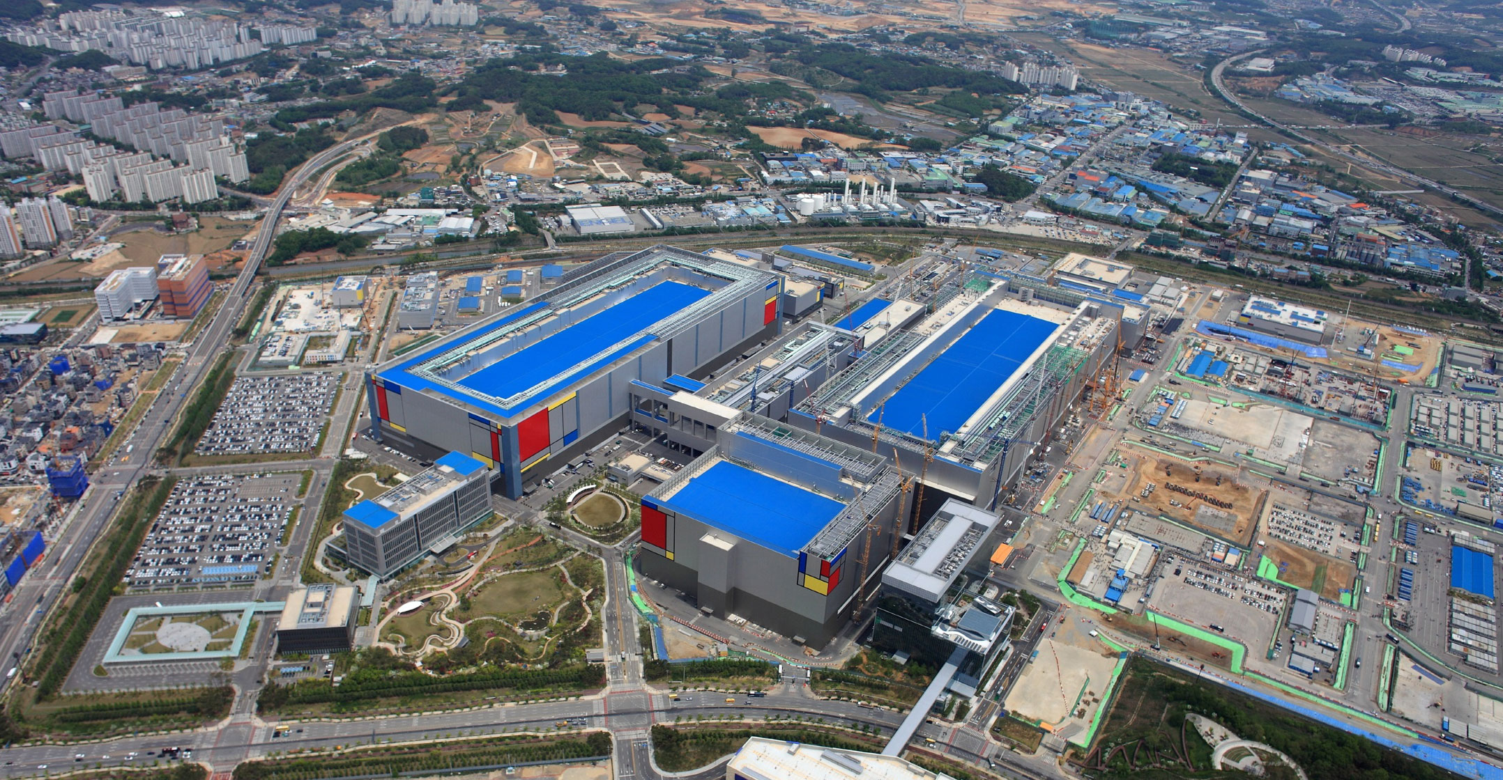
Samsung started up its first dedicated plant for EUV-based fabrication in the southern city of Hwaseong this year, while a second facility in Pyeongtaek is slated for mass production in the second half of 2021. The growth rate of its foundry business is expected to significantly exceed that of the market, which is likely to be in the high single digits, Shawn Han, senior vice president of the semiconductor business, said during a recent earnings call. The GAA technology that Samsung’s chosen is expected to be adopt by TSMC for 2nm processes in 2024, but there’s a chance that schedule could be moved up to the second half of 2023, said Kim Young-soo, an analyst at SK Securities.
“Technically, Samsung could turn the table in 2023 before TSMC kicks off the 2nm production,” Kim said. “There will be overflow orders of making application processor chips and edge computing devices. The key to expand the market share is how many EUV machines Samsung can secure.”
Officials at Samsung believe the company has a competitive edge from its experience building both the chips and the devices that they go into, like Galaxy smartphones. It can foresee and address the engineering requirements of its clients. Samsung believes its other trump card is an ability to package memory and logic chips into a single module, improving power and space efficiency. But some companies may be wary about outsourcing production to a direct competitor. TSMC executives have from time to time highlighted the fact that the Taiwanese chip maker doesn’t compete with any of its customers, a clear jab at Samsung. — Reported by Sohee Kim, (c) 2020 Bloomberg LP


