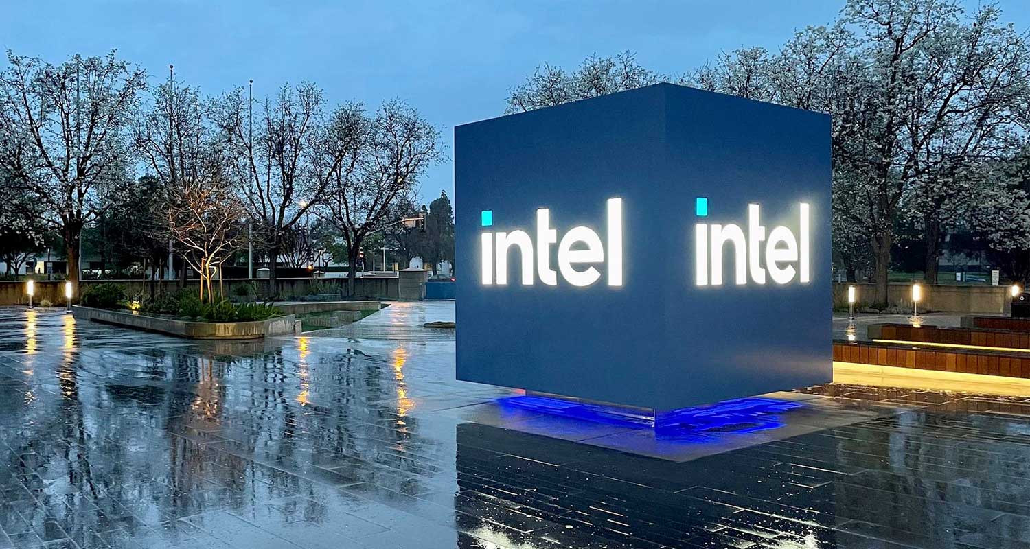
 Intel is betting on an unexpected material to help the world’s computers handle ever-growing artificial intelligence workloads: glass.
As processors become larger and more complex, their ability to communicate with the rest of the computer is going to become a chokepoint, according to Intel researchers. Glass-based substrates, which sit between the chip and connecting components, are the answer to this challenge, the company says.
For Intel, a chip pioneer that’s now chasing Nvidia for the limelight, the new approach is a chance to show off its ability to innovate for an AI world — and win new customers in the process. The company has ramped up R&D spending to nearly US$18-billion/year, well ahead of its peers.
Intel’s glass push is coming from its packaging research and production facilities, a little-known part of its technology line-up. The Santa Clara, California-based company is trying to raise the profile of the business, part of a broader effort to attract customers to its manufacturing operations.
Since Intel was founded in the late 1960s, its factories have concentrated on almost exclusively producing its own designs. Now the chip maker is building up its foundry operations, which make semiconductors and other technology for outside customers — one of the biggest shake-ups in the 55-year-old company’s history.
CEO Pat Gelsinger has been increasingly talking up Intel’s capabilities in packaging — the technology that surrounds chips. And the company is making headway in signing up customers in that area, he says, even if those buyers bring chips that were made elsewhere.
Intel’s high-stakes bet
The packaging business is seen as a way to lure in clients, who may then use Intel for a broader swathe of their chip-making needs. It’s a high-stakes bet. Intel is spending billions on new plants around the world, with the hope that outside customers will keep them humming along.
Gelsinger, who will headline Intel’s annual technology conference later this week, also is trying to restore the idea that the company can set the agenda for the $580-billion chip industry.
With the glass packaging initiative, Intel aims to be the first to commercialise a technology that’s been in academic research for years. The chip maker anticipates that existing techniques will run out of steam in the second half of this decade, creating an urgent need for new solutions.
The tiny metal paths that carry data and power between the billions of transistors on a chip and the rest of the computer have to pass through a package that protects the silicon. For the last 20 years, that substrate has been made of a mixture of fibreglass and epoxy. The material is relatively cheap and has become an industry standard.
As chips encompass tens of billions of transistors and more, fuelled in part by the demands of AI software, that packaging layer is showing its limitations. The tiny electronic components need to be clamped down with a force equivalent to a rugby player sitting on them — otherwise, the electrical contacts don’t touch cleanly.
Increasing the number of holes in the flexible substrate leads to warping, which can cause loss of contact in some areas. The epoxy and fibreglass mixture also limits how much the pathways for power and data can be scaled down.
Glass fixes those problems, Intel says. The material doesn’t warp, and its structure allows for the use of more finely cut pathways for data. The material shares chemical properties with the silicon it’s supporting, meaning it will expand and contract at the same rate in high temperatures.
But it’s no sure thing. Before the approach goes mainstream, Intel will need to get a cheaper supply of material. And researchers need to refine handling techniques to guard against glass’s most famous characteristic: its tendency to shatter. — (c) 2023 Bloomberg LP


